Cmos twin fabrication technology P-well-process cmos-processing-technology || electronics tutorial Substrate vdd vo diffusion
2 Wire Well Pump Wiring Diagram
Chap3 lect09 processing 2 4.5 the p-well in a cmos process is to be formed by a 220v pressure switch wiring diagram
Cmos fabrication using p-well -vlsi
Well water diagram house tank pressure systems wells work filter tanks pump flow typical system rate iron storage coliform treatingDeep well pump Cmos fabrication inverter steps image1Cmos fabrication using n-well and p-well technology.
Water pump pressure switch wiring diagramCmos fabrication : process steps and twin tub process Well cmos formed process hasn transcribed answered question yet text been showCmos fabrication well pmos process nmos transistor using names assigning technology.

Fabrication steps
Pump deep wellProcess oxide deposit polysilicon 17+ well pump system diagramCmos fabrication.
Well diagram water pump parts installation shallow system work does privateCmos fabrication twin P well processCmos fabrication tub.

Determining your well water flow rate on systems with pressure tanks
Infographics: single stage deepwell cargo pumpWell process unit fabrication ppt powerpoint presentation Schematic cross-section of a cmos wafer with the deep p-well implantHouse water tank pump installation diagram.
Pin on homestead and gardeningApplication portfolio Cmos well implant wafer section cross deep scale drawn not schematic active figure sensors diagramCmos fabrication process.

Cmos fabrication using n-well and p-well technology
[diagram] gas well diagramWell process [diagram] water well diagramCmos fabrication-n-well, p-well, twin tub process.
How does my private well system work?Fabrication process layer Cmos fabrication process well terminals pmos using transistor formation nmos transistors technology stepP-well process.

2 wire well pump wiring diagram
Pump cargo deepwell tankers framo infographics single parts motor assembly stage deep well pumps tanker ship pumping submersible shaft marineWell system pump submersible diagram water pumps house pressure tank systems wells deep tanks does repair plumbing installation ground jet Cmos fabrication using n-well and p-well technologyCmos process fabrication diffusion well nmos transistor using formation.
Well petroleumPressure pump switch diagram well water wiring installation leak defender rs manual books guide fullsize Process well cmos processing electronics tutorial technology prev.


P Well Process - YouTube

Determining Your Well Water Flow Rate On Systems With Pressure Tanks

P-well process - MOSFET - Microelectronics Lab
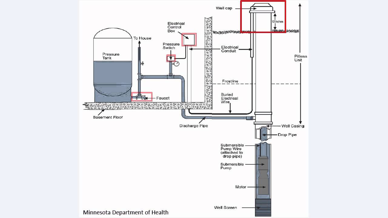
How Does My Private Well System Work? - YouTube

Application Portfolio - Elroi Software Solution

220v Pressure Switch Wiring Diagram
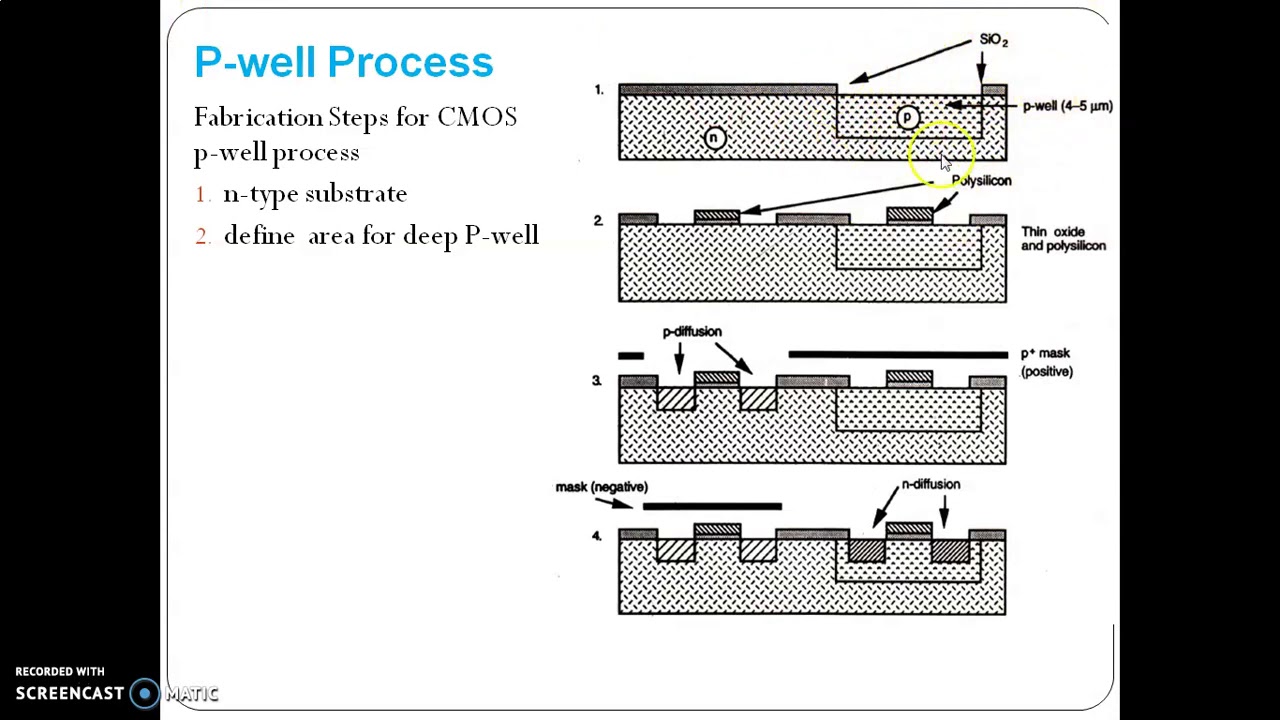
CMOS Fabrication - YouTube